 2025/02/19
Background knowledge
In modern semiconductor manufacturing processes, the quality of the wafer directly determines the performance and yield of the chip. Even a slight deviation in the thickness of the wafer may cause a series of problems in subsequent processes, such as circuit short circuits and signal transmission delays.
Traditional thickness measurement methods are gradually unable to meet the increasingly stringent industrial needs in terms of accuracy, efficiency and adaptability. The 3D camera wafer through-beam thickness measurement technology came into being. With its unique advantages, it has brought a new solution to wafer thickness measurement.
Camera model selection
Today, I would like to introduce the application cases of Yishi Technology's LVM2520 and LVM2330 line laser 3D cameras in semiconductor manufacturing inspection!
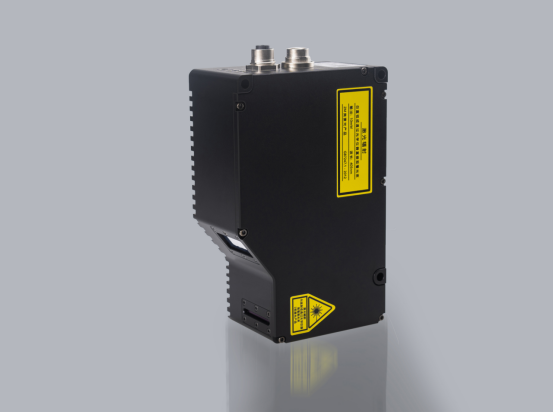
The LVM2520 3D intelligent sensor has a full-frame acquisition rate of 2500Hz, and the highest rate can reach 56000Hz by setting the ROI; it has 1920 physical contour points, and the highest number of points can reach 4096 under the condition of uniform spacing sampling of the depth map. The comprehensive performance of the product is at the leading level in the industry and is an ideal choice for high-speed online inspection systems!
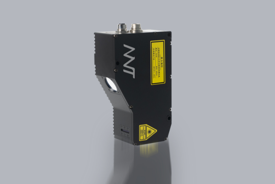
LVM2330 3D intelligent sensor. Its full-frame acquisition rate is 1000Hz. Through setting ROI, the highest rate can reach 20000Hz. There are 1920 physical contour points. Under the condition of uniform spacing sampling of the depth map, the highest number can reach 4096 points, which meets the needs of various high-speed and large-batch detection applications!
Detection item

Workpiece information
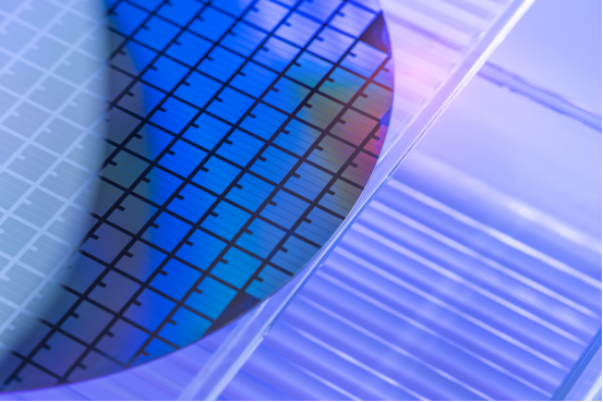
·Material: Silicon wafer
·Color: White
·Size: 190×140mm
Inspection requirements
·Inspection item: Thickness detection
·Repeatability precision: 6um
·Speed requirement: Greater than 150mm/s
Detection environment and installation methods
·Scanning method: The camera is fixed, and the test sample moves along the central straight line for scanning and measurement.
·Triggering method: The encoder is used for triggering, and a stable AB phase differential signal is output.
·Communication method: TCP/IP Ethernet.
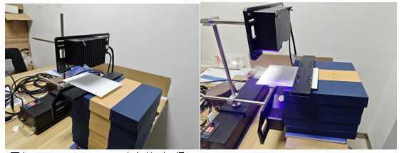
*The picture shows the detection site of LVM2520 and LVM2330 cameras.
Pick picture effect
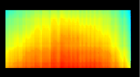
·The picture shows the rendered effect diagram of the product point cloud.
Measurement data
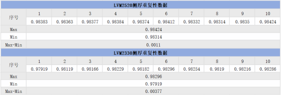
·The maximum ten-group static repeatability of LVM2520 is 0.0011mm, and the maximum ten-group static repeatability of LVM2330 is 0.0038mm.
Inspection conclusion
This test uses 3D camera LVM2520 and LVM2330 blue laser camera. Both cameras meet the test requirements.
The maximum frame rate of LVM2520 in the test is 17000fps, and the theoretical maximum speed is 272mm/s (excluding the mechanism movement time). The maximum value of ten groups of static repeatability is 0.0011mm.
The maximum frame rate of LVM2330 in the test is 9000fps, and the theoretical maximum speed is 288mm/s (excluding the mechanism movement time). The maximum value of ten groups of static repeatability is 0.0038mm.

