 2026/06/26
background knowledge
Slotted copper plates serve as essential components for smartphone VC heat dissipation plates, fast-charging conductive modules, and laptop power supply connection substrates. Variations in copper plate thickness can directly lead to batch-wide quality issues such as inadequate device cooling, excessive electrical resistance, and improper assembly gaps. Addressing the industry challenge of traditional inspection methods failing to meet modern mass-production demands, Next Vision Tech's LVM3422 3D linear laser camera offers a comprehensive solution. Through specialized hardware and algorithm optimization, it enables full-range integrated thickness detection for VC slotted copper plates on high-speed automated production lines.
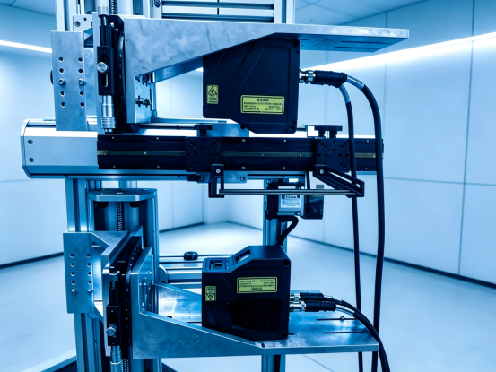
Key pain points in industry monitoring:
|
Copper materials exhibit high reflectivity, making their slotted edges prone to overexposure; conventional laser sensors produce significant point cloud noise and result in contour edge loss. |
|
The coverage rate of random sampling inspections is insufficient, making comprehensive testing impossible and posing high risks to quality control. |
|
2D vision lacks Z-axis three-dimensional height data, making it unable to perform thickness quantification detection; general-purpose laser sensors exhibit poor repeatability and fail to meet the stringent tolerance requirements for ultra-thin copper plates. |
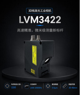
Model | LVM3422: Core Hardware Advantages of a Line Laser 3D Camera
• Ultra-high-density contour sampling: The depth map achieves uniform sampling of up to 3,200 points per frame, accurately reproducing the contours of fine grooves and slots.
• Wide-format high-speed scanning capability: Acquisition frame rate ranges from 2000 Hz to 30,000 Hz, with continuous stable scanning at 2000 Hz for full-frame applications; compatible with high-speed production lines in the 3C and new energy sectors.
·High-dynamic imaging hardware optimization: Specifically suppresses overexposure in high-brightness copper areas while fully preserving details at groove bottoms, addressing common issues of noise in point clouds and edge loss associated with highly reflective copper surfaces.
·Self-developed hardened sub-pixel edge detection algorithm: achieves a static repeatability accuracy of 0.6 μm, enabling precise extraction of complete groove contour boundaries
Project Testing Requirements
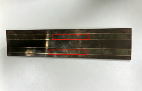
· Inspection of workpiece: VC uniform heating plate with slotted copper plate, width 40 mm
· Testing items: Comprehensive thickness measurement of both sides of the copper plate; measurement of thickness from the red-marked area to the back surface.
· Customer tolerance requirements: repeatability accuracy for thickness measurement ≤ 0.02 mm
Practical Performance: Dual guarantees of safety and reliability
(1) Image Capture Results
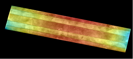
The image shows the front brightness map and point cloud.
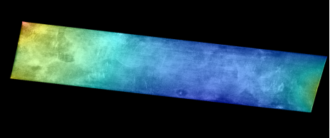
The image shows the backlight brightness map and point cloud map.
(II) Measured thickness repeatability data (from 10 consecutive samples)
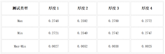
Actual measurement results of the project
The entire dual-camera alignment system achieves a maximum static repeatability of only 5.2 μm and a maximum measurement range across all categories of merely 0.0052 mm.
·Customer-specified tolerance: 0.02 mm; measured accuracy significantly exceeds requirements, with ample process tolerance allowance provided
·Single-camera Z-axis detection accuracy: ±0.003 mm; dual-camera cross-beam thickness measurement achieves a combined accuracy of ±0.006 mm
(3)Production Line Adaptation Efficiency Indicator
|
project |
test result |
|
Imaging Quality
|
The point clouds on both sides of the high-reflection copper plate are clean and free from noise; the edges of grooves, bends, and joints exhibit sharp contours, with stable micron-level height deviations. |
|
scanning speed |
Under the current project configuration—with a 40 mm field of view in the X direction, a 6 mm field of view in the Z direction, and a resolution of 16 μm—the actual achievable stable scanning speed is 104 mm/s, matching the production line's current rhythm. |
|
Field of view coverage |
Proximal end: 36 mm; distal end: 48 mm, fully covering a 40-mm-wide copper plate workpiece without requiring multiple segmented scans. |
|
Feasibility of the Solution |
Supports comprehensive integrated automatic thickness measurement for copper plates, enabling full inspection to replace manual sampling and contact-based thickness measurement equipment. |
The core competitiveness of the Yishi LVM3422 solution
· Specialized anti-glare optimization: Combines hardware-based high-dynamic imaging with proprietary chip-hardening algorithms, delivering optimal performance in copper high-gloss surfaces and addressing industry-wide imaging challenges.
• Micrometer-level stability accuracy: Static contour precision of 0.6 μm, significantly exceeding the tolerance standards for 3C VC copper boards;
• High-speed, comprehensive integrated inspection: A single scan completes full-thickness inspection of the entire board; a stable scanning speed of 104 mm/s is ideal for automated mass production.
·Domestic alternative solution: The LVM series features self-developed hardware and software with a maximum repeatability accuracy of 0.1 μm, matching or surpassing performance of overseas counterparts while reducing corporate equipment procurement costs.
In addition to VC uniform heating plate slotted copper plates, the LVM3422 can simultaneously handle various precision copper material inspection tasks, including fast-charging conductive copper bars and laptop connection copper contacts. For applications requiring micron-level dimensional, thickness, or contour measurements of ultra-thin metal components or highly reflective parts, contact Next Vision Tech for customized 3D visual measurement solutions to reduce production line defect rates and achieve fully automated precision quality control.


 浙公网安备33021202004092号